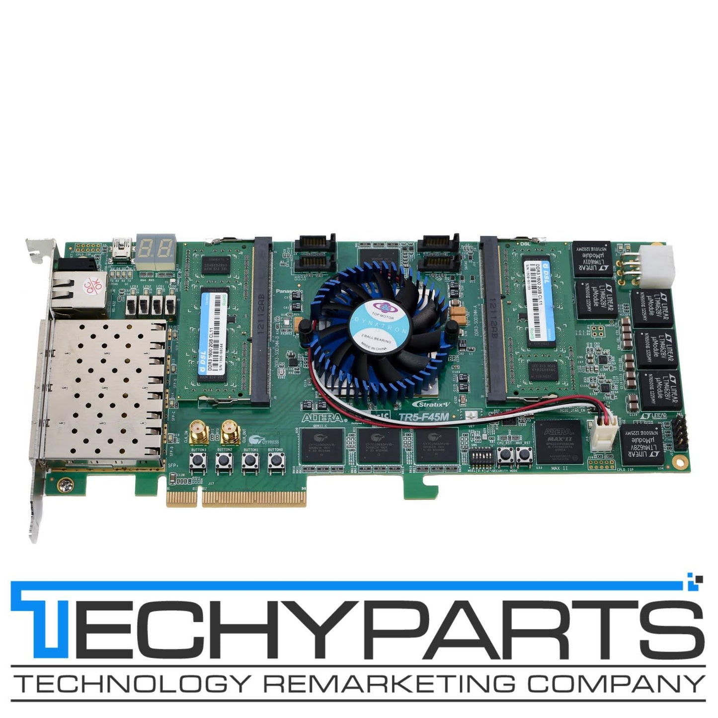
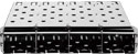
Terasic DE5-Net TR5-F45M Altera Stratix V GX FPGA PCI-E x8 Development Board
85685Terasic DE5-Net TR5-F45M Altera Stratix V GX FPGA PCI-E x8 Development Board

Terasic DE5-Net TR5-F45M Altera Stratix V GX FPGA PCI-E x8 Development Board
Terasic DE5-Net TR5-F45M Altera Stratix V GX FPGA PCI-E x8 Development Board with 4GB (2x 2GB) DDR3 SODIMM Memory
Manufacturer: TERASIC
TERASIC Model Number: DE5-NET
TERASIC Part Number: TR5-F45M
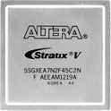
FPGA Series: Altera Stratix V GX FPGA (5SGXEA7N2F45C2)
This part is a working pull. It has been tested by a qualified technician.
You will receive this part as pictured. No software, licensenses, parts or accessories other than those mentioned or pictured in the listing will be included.
30-Day Warranty!
Manufacturer's description and specifications:
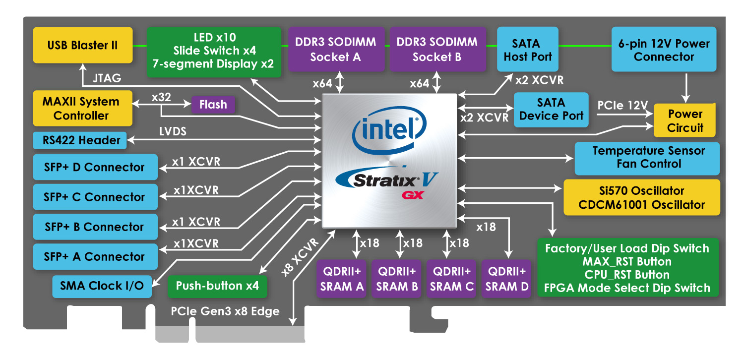
The Terasic DE5-Net Stratix V GX FPGA Development Kit provides the ideal hardware solution for designs that demand high capacity and bandwidth memory interfacing, ultra-low latency communication, and power efficiency. With a full-height, 3/4-length form-factor package, the DE5-Net is designed for the most demanding high-end applications, empowered with the top-of-the-line Altera Stratix V GX, delivering the best system-level integration and flexibility in the industry.
The Stratix® V GX FPGA features integrated transceivers that transfer at a maximum of 12.5 Gbps, allowing the DE5-Net to be fully compliant with version 3.0 of the PCI Express standard, as well as allowing an ultra low-latency, straight connections to four external 10G SFP+ modules. Not relying on an external PHY will accelerate mainstream development of network applications enabling customers to deploy designs for a broad range of high-speed connectivity applications. For designs that demand high capacity and high speed for memory and storage, the DE5-Net delivers with two independent banks of DDR3 SO-DIMM RAM, four independent banks of Cypress QDRII+ SRAM or functional compatible SRAMS provided by GSI and ISSI, high-speed parallel flash memory, and four SATA ports. The feature-set of the DE5-Net fully supports all high-intensity applications such as low-latency trading, cloud computing, high-performance computing, data acquisition, network processing, and signal processing.
FPGA
 |
FPGA
Altera Stratix® V GX FPGA (5SGXEA7N2F45C2)
FPGA Configuration
On-Board USB Blaster II or JTAG header for FPGA programming
Fast passive parallel (FPPx32) configuration via MAX II CPLD and flash memory
|
Memory
 |
Memory
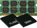
Two Independent DDR3 SODIMM Socket, Up to 8GB 800 MHz or 4GB 933 MHz for each socket
Four Independent 550MHz SRAM, 18-bits data bus and 72Mbit for each
256MB FLASH
|
Communication
 |
Communication Ports
Four SFP+ connectors
PCI Express (PCIe) x8 edge connector (includes Windows PCIe drivers)
One RS422 expansion header
|
Others
 |
General user input / output:
4 LEDs
1 LED Array
4 push-buttons
4 slide switches
2 seven-segment displays
SMA clock input / output
On-Board Clock
50MHz Oscillator
Programmable oscillators Si570, CDCM61001 and CDCM61004
System Monitor and Control
Temperature sensor
Fan control
Power
PCI Express 6-pin power connector, 12V DC Input
PCI Express edge connector power
Mechanical Specification
PCI Express standard height and 3/4-length
|
Block Diagram